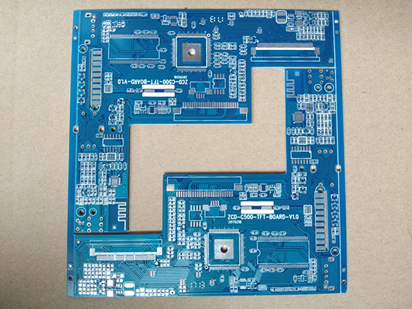
Several Reasons for Poor Tin on PCB Tin Surface
Circuit Board Manufacturer This paper summarizes some viewpoints about tin defect on PCB tin surface. We can refer to them and hope to help us. The main factors that cause poor soldering of PCB board are from two aspects: PCB factory and SMD factory:
1. Storage environment and transportation: This is the link between the manufacturers of dielectric circuit boards and patch factories. Generally, there are few inventories of PCBs. However, the general inventory requires that the storage environment should be suitable for dry and humid conditions, and the packaging should be intact. In the process of transportation, it is necessary to handle as lightly as possible. Vacuum packaging should not be allowed to be damaged and stored for a long time, and tin spraying board management should be allowed. The time of storage is one month, but the best time of solderability is within 48 hours. If the time of storage exceeds one month, it is advocated to come back to the PCB factory to clean and bake the PCB with special medicines. Baking parameters 150 1 hour
2. Operation does not comply with the operation standards when shipment: the line occupation is a workshop environment, the standard operation requirements of workers are extremely strict, especially in the production of circuit boards are chemical reaction environment, so impurities are not allowed to enter. After the board tin spraying process is completed, a series of follow-up needs workers to wear. Anti-static glove operation, because finger sweat or stains directly touch the appearance, will form surface oxidation, if the formation of bad extremely difficult to find, and irregular presentation, testing and tin test are difficult to expose.

3. Welding defects caused by warping: warping occurs in the welding process of circuit boards and components, and virtual welding and short circuit occur due to stress and deformation. Warpage is often caused by the temperature imbalance between the upper and lower parts of the circuit board. Large PCBs can also warp when they fall due to the weight of the board itself. Ordinary PBGA equipment is about 0.5mm away from PCB. If the equipment on PCB is large, the solder joints will be under stress for a long time as the PCB recovers its normal shape after cooling down. If the equipment is raised by 0.1mm, it will lead to virtual soldering open circuit. For special products, it can be required that the Yin-Yang patchwork of PCB factory is beneficial to reduce warping. Music, maybe take the appropriate size of the patchwork, not too large, not too small.
4. Source of tin for incoming materials: With regard to material acquisition, some PCB factories are blindly pursuing tightening costs. When using tin-sprayed raw materials, some PCB factories collect tin from their purchasing profession. Ordinary PCB factories with very low unit price may have such dangerous chances. We advocate that we carefully select suppliers.
5. Tin-spraying furnace not timely slag removal finishing: Tin-spraying furnace on time maintenance is very important, because tin-spraying is a vertical cycle process, PCB board surface will be under strong pressure, about those boards that are not solderproof, not strong characters, will occur impact lead to falling off, deposited in the furnace, through high temperature transpiration, if too much. All the time, it is not tidied up to form external adhesion.
The article originated from Jiangmen single-sided and double-sided circuit boards. http://www.yonghongpcb.com
-
07-18
What is the structure of blind buried hole circuit board?
Blind buried-hole circuit boards have the characteristics of free zigzag, folding and winding, free movement and expansion in three-dimensional space, good heat dissipation performance and high precis
-
07-18
What role does copper play in circuit boards?
PCB manufacturers take you to know that there are several reasons for PCB copper laying: 1. EMC can shield large area of ground or power supply copper, and some special areas, such as PGND, play a pr
-
07-18
Four matters needing attention in choosing PCB manufacturer
When choosing PCB manufacturers, the price of PCB manufactured by professional manufacturers will be more affordable, and the quality assurance will be stronger, which will be more guaranteed after
-
07-18
How to use three glue-proof PCB correctly?
Sanfang gum does not contain evaporative substances such as acetone and xylene, which is more environmentally friendly and safe. Mainly used in electronic circuits and components to form a protectiv